 |
Introduction to VLSI Systems (6.371)
12/11/2002
|
 |
Each cluster in the DXC executes instructions which can operate on local data values, and also send and receive values on the transport network. A central feature of the Dataflow Execution Core is the dynamic resolution of dependencies when two clusters communicate. The dynamic dataflow is accomplished using dedicated send and receive signals to connect every pair of communicating clusters. When a cluster is ready to send data to another cluster, it broadcasts the data on its output bus and asserts the appropriate send signal; likewise when a cluster is ready to receive data from another it asserts the appropriate receive signal. When both signals are asserted, the two clusters simultaneously detect that the data transfer has completed.
Figure 3 shows a pipeline diagram of the cluster. The pipeline has three stages: decode (D), execute (X), and writeback (W); and each stage has two phases: clock high (h), and clock low (l). A new instruction is clocked into the instruction register (IR) at the beginning of the decode stage. During Dh the register file bit-lines precharge while the source register specifiers are decoded, and two registers are read and latched (in X and Y) during Dl. During Xh, a mux selects the ALU/shifter inputs, and these are latched (in S and T) and sent to the ALU to initialize the carry chain. The ALU's dynamic carry chain evaluates during Xl, and a mux selects between the ALU and shifter for the X stage result latch (R). This value can be bypassed to the following instruction, or written back to the register file during Wh (in time for the second following instruction to read the register during Dl). A result value can be latched (in Xo) at the beginning of Wh to be transported to another cluster during Wh and Wl. A received transport value enters the pipeline (in Xi) during Dl for input to arithmetic operations. Therefore, the pipeline allocates almost a full clock cycle to allow transport operations to complete.
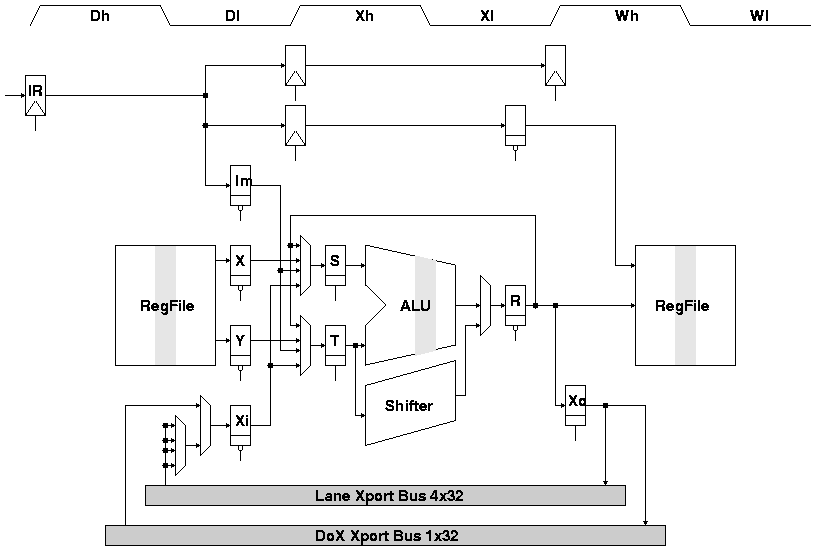 |
The DXC pipeline has two stall conditions. An instruction stalls in stage D if it has a transport receive operation for which the data is not yet available. The stall is accomplished by not clocking a new instruction into the instruction register, and sending a pipeline bubble into stage X. If a transport send operation has not completed by the end of stage W, then the instructions in D and X must be stalled if the instruction in stage X also contains a transport send operation. In this case, the result of the stage X instruction is preserved in the R latch by gating its clock on the following cycle. Writeback operations to the register file are never stalled after an instruction enters stage X.
I created a cycle-accurate behavioral DXC simulator using the Sychosys simulation framework. The Sychosys structural netlist files [ cluster.sychonet, lane.sychonet, DXC.sychonet ], behavioral C++ models [ SychoBlock_DXC.h, SychoBlock_alu.h, DXC_Block_ALU.h, SychoBlock_shifter.h ], and simulation driver code [ testdxc.cc, DXC_Instr.h, DXC_Instr.cc ] are provided for reference.
The datapath uses a bit-slice layout strategy in which each bit has a height of 54λ, enough space for 6 metal-3 routing tracks. Figure 4 shows 3 bits of a 4-input mux as an example. The datapath cells use metal-1 and metal-2 for internal routing, and metal-3 is used to connect the datapath modules together. To simplify the routing task, I extended the datapath modules with input and output "landing pads". As shown in Figure 4, these are strips of metal-2 which extend across the height of the bit-slices so that a connection can be made to any metal-3 track by simply adding a via.
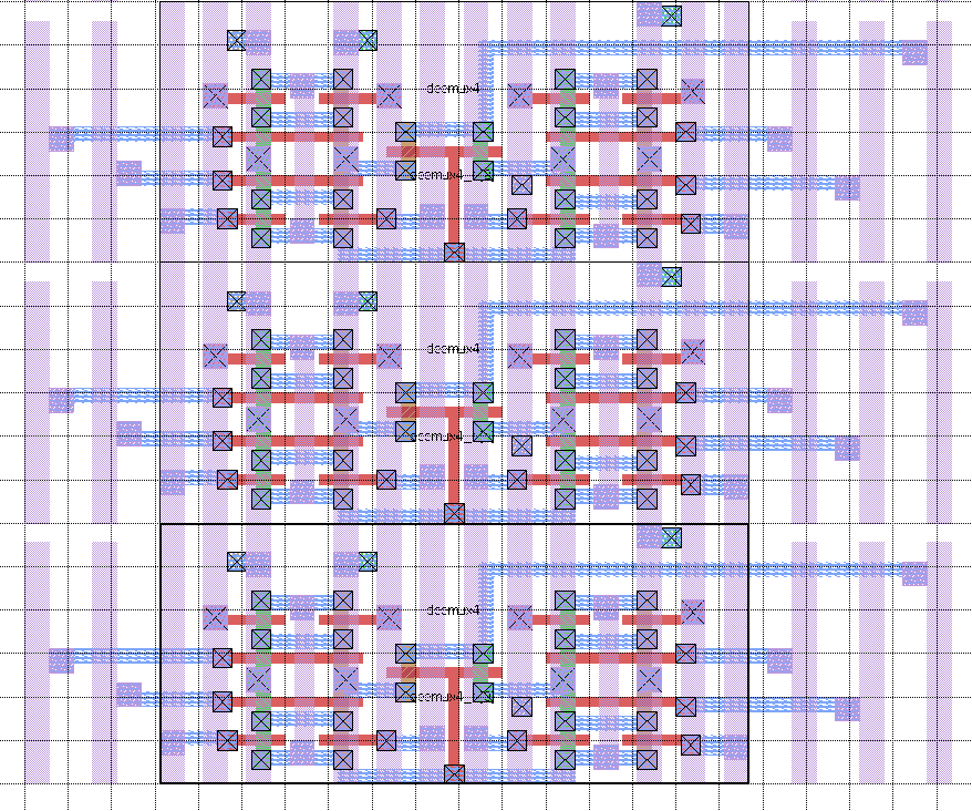 |
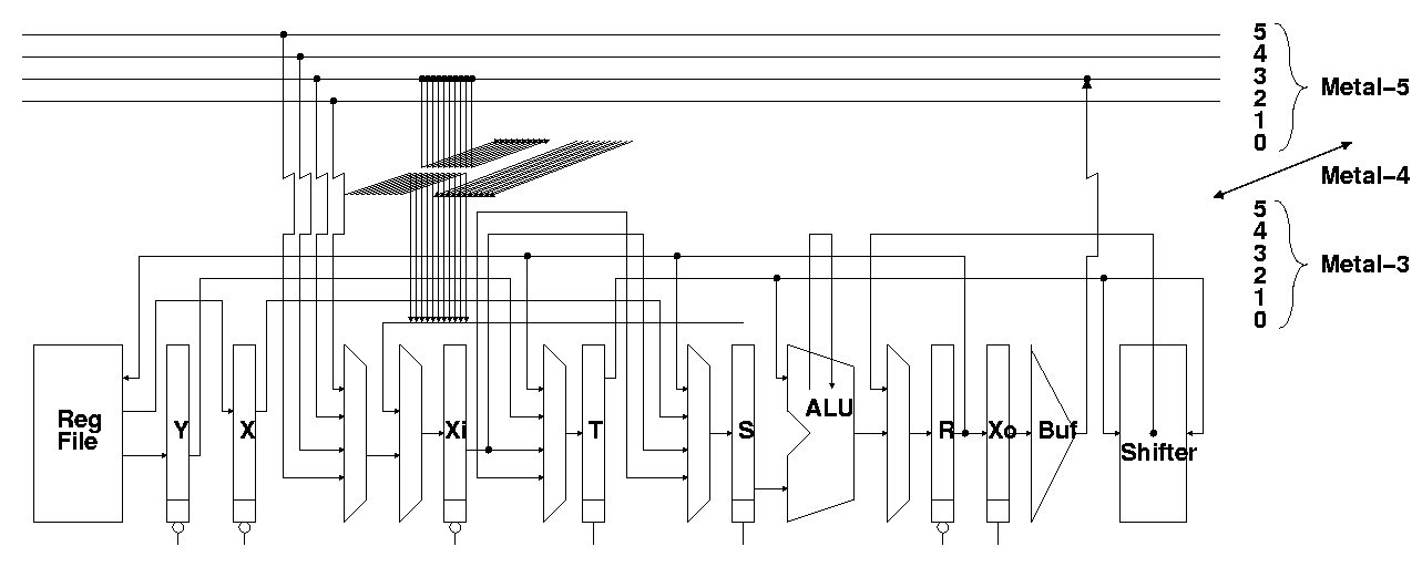
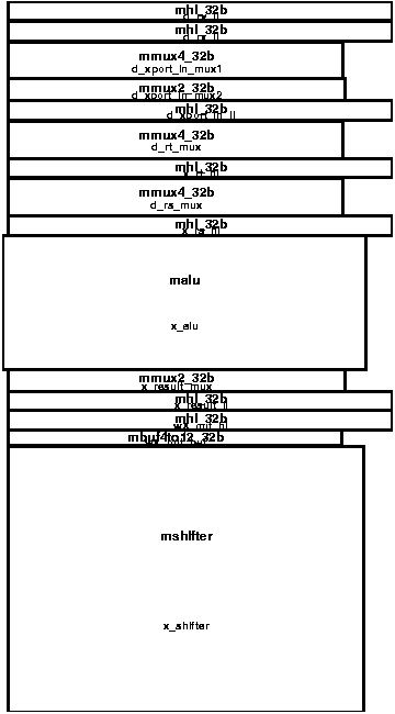
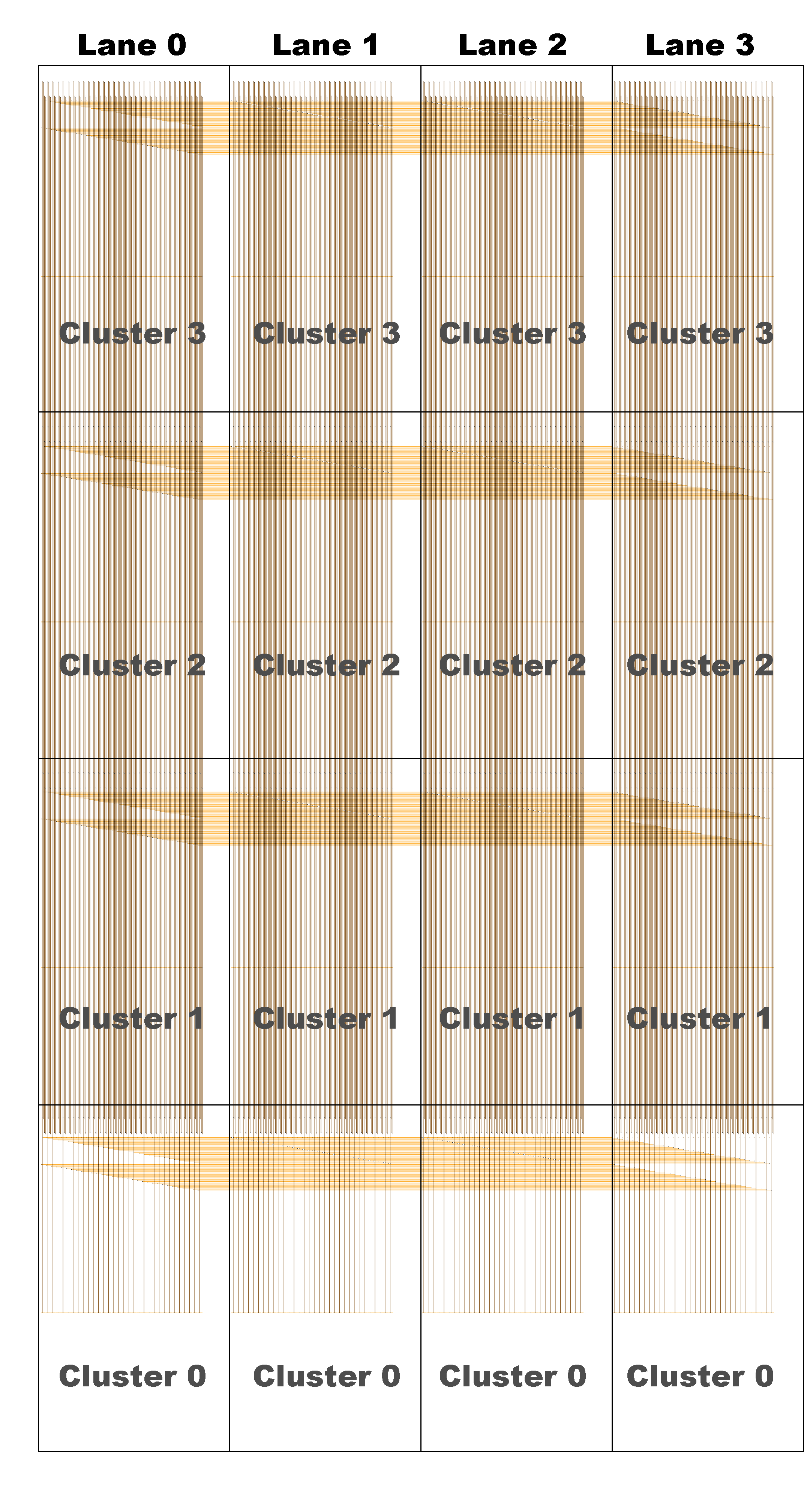
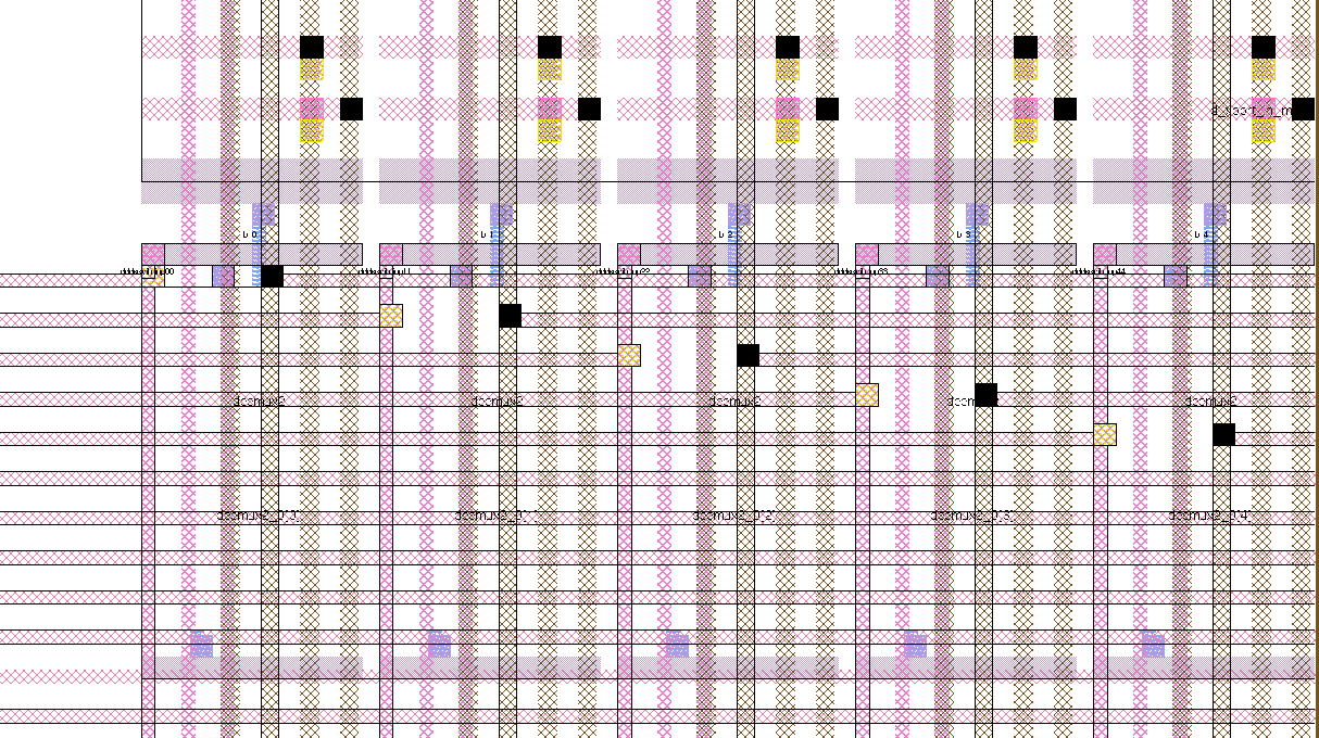
Figure 5 shows the placement and routing track allocation strategy for the cluster datapath. The datapath cells shown represent a single bit-slice, and the routing above the cells shows the track allocation. Connections between neighboring cells can use a "sneak path" and avoid using a metal-3 track. Figure 6 shows the placed and routed cluster layout with different sub-figures for each metal layer. Note that this layout is rotated 90 degrees to the right compared to Figure 5. Figure 7 shows a floorplan of the entire DXC array of clusters together with the lane and do-across transport routing. The dimensions of a cluster are 2022λ x 3675λ, or 0.25mm x 0.46 mm; the entire DXC is 1.0 mm x 1.8 mm. Each cluster contains 10,328 transistors, for a total of 165,248 transistors in the entire DXC.
 |
 |
 |
 |
 |
 |
 |
 |
 |
 |
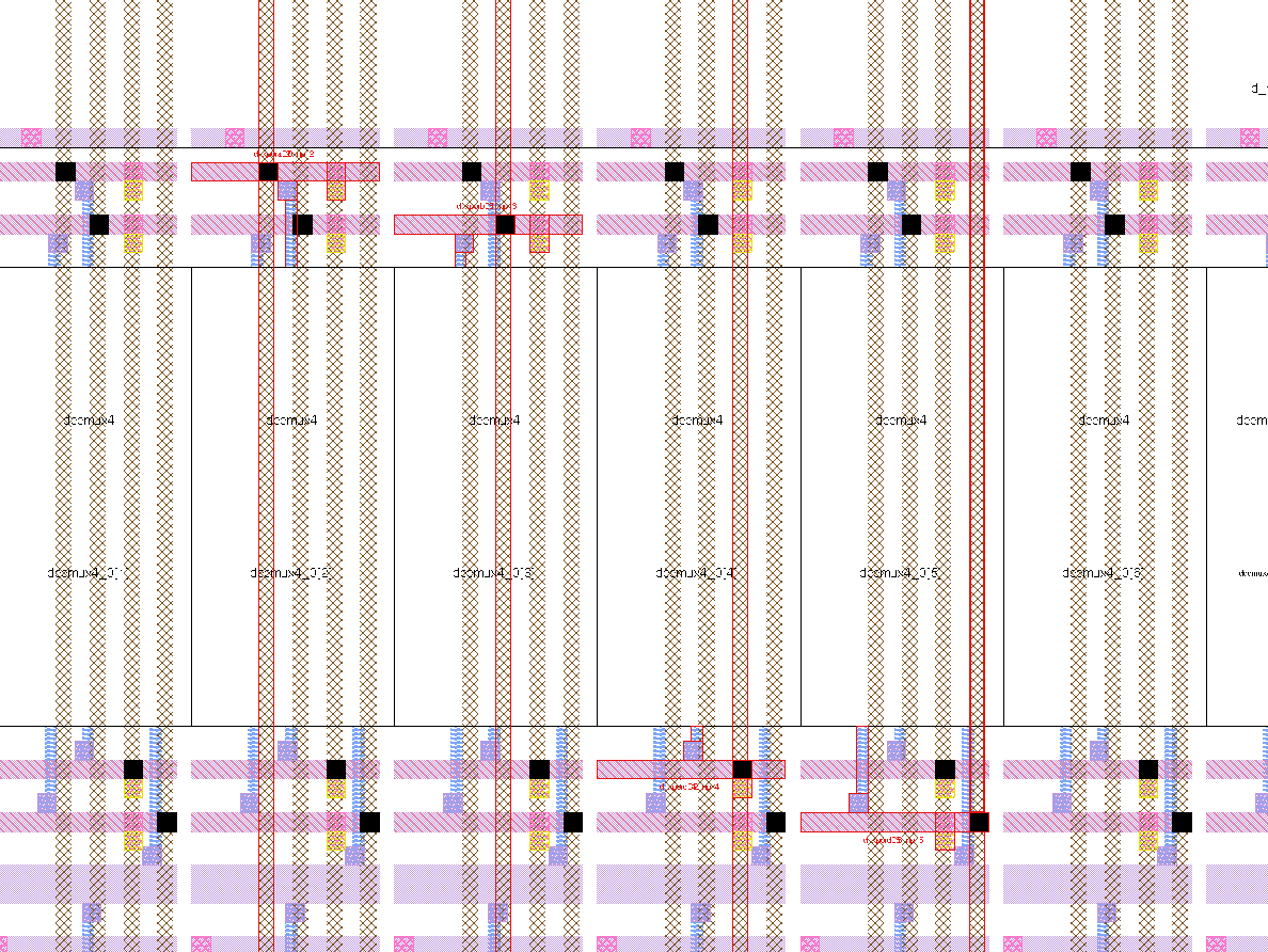
Due to the limited number of metal-3 tracks in the datapath cells, the four lane transport busses use metal-5, as shown in Figure 5. To make these input and output connections, a short segment of a metal-3 track is used to jump up to metal-4 and create a landing pad directly above the metal-2 landing pad for the datapath cell. Then, any metal 5 track can connect to the pad by adding a via. Figure 8 shows the connections between the lane transport busses and the input mux. One connection for each of the four lane transport bus is highlighted in red (in four adjacent bit slices).
The do-across transport busses between neighboring clusters use metal-4. The connections between Lane 0 and 1, Lane 1 and 2, and Lane 2 and 3, all use the same 32 metal-4 tracks; and the connection from Lane 3 back to Lane 0 uses an additional 32 metal-4 tracks. As shown in Figure 5, the incoming do-across bus to a cluster connects down to metal-3 on track 0 (the left-most track in Figure 7). The outgoing do-across bus connects to the appropriate lane transport bus on metal-5; the lane-transport busses use tracks 2 through 5 so that the incoming and outgoing do-across busses can use the same metal-4 tracks without conflicting. An example section of the do-across bus ripping is shown in Figure 9. In this figure, the incoming do-across bus from the left connects to metal-3 on track 0, and the outgoing do-across bus connects to metal-5 on track 3.
 |
 |
The C++ code [ SP_build_cluster.cc, SP_build_lane.cc, SP_build_dxc.cc ] used along with the Spongepaint library to generate layout for the cluster, lane, and DXC, is provided for reference.
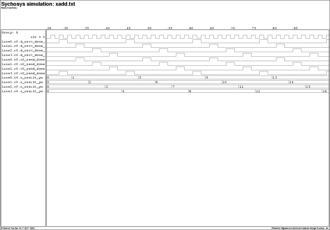
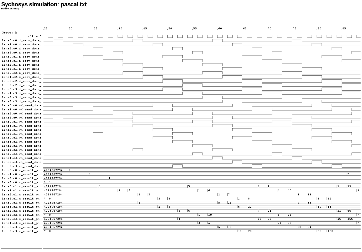
The test programs were run using the behavioral DXC simulator. Correct behavior was verified by analyzing a dump of all the register values at the end of each simulation. These simulations produce VCD (value-change dump) trace output which tracks the values on all the nets in the behavioral DXC model for every simulated clock phase (twice per cycle). The VCD output can be displayed in a waveform viewer, and examples are shown in Figure 10 for the xadd.txt program, and in Figure 11 for the pascal.txt program. Figure 10 shows the send_done and recv_done control signals and the output of the X state result latch for cluster 0 on all the lanes. The computation can be seen to ripple around the do-across network as the instructions' dataflow dependencies resolve dynamically. Figure 11 shows the same signals for all the clusters. The results show that each row of clusters in the DXC compute a diagonal of Pascal's triangle ({1, 1, 1, 1, ...} on cluster 0, {1, 2, 3, 4, ...} on cluster 1, {1, 3, 6, 10, ...} on cluster 2, and {1, 4, 10, 20, ...} on cluster 3).
 |
 |
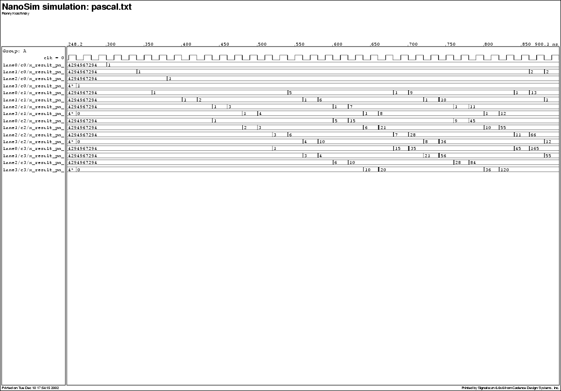
To test the layout, a spice netlist was extracted from the final layout representation. A script was used to convert the VCD trace from the behavioral simulator into stimulus files to drive the external inputs of the extracted layout, and to check that all the internal nets had the correct values every cycle. The NanoSim tool from Synopsys was used to run this simulation, and it flagged any differences between the behavior of the extracted layout and the expected net values. NanoSim also generated a trace of the net values which could be compared to the behavioral simulation. Figure 12 shows an example for the pascal.txt program, and the values can be verified to match those of Figure 11. The send_done and recv_done control signals are not shown because the extracted layout does not include any control logic.
 |
Using this infrastructure, the extracted layout of the ALU and shifter were verified by running several thousand cycles of directed tests. Both the extracted layout for a single cluster and the extracted layout for the entire DXC were verified by running the four test programs listed above. For all test cases, the behavior of the layout matches the behavioral model.